ASML EUV Breakthrough: 1000-Watt Light Source to Boost Chip Production 50% by 2030
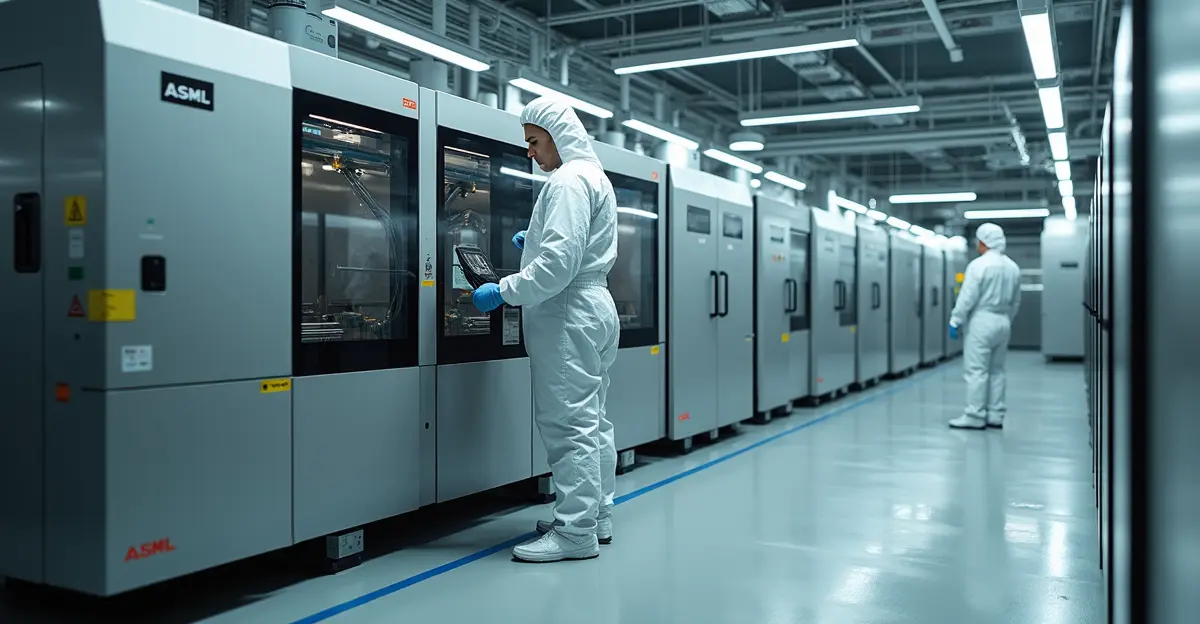
Dutch semiconductor equipment giant ASML has unveiled a groundbreaking advancement in extreme ultraviolet (EUV) lithography technology that could increase chip production by up to 50% by 2030. The Veldhoven-based company announced in February 2026 that it has successfully boosted its EUV light source power from 600 watts to 1,000 watts, representing a significant leap forward in semiconductor manufacturing efficiency that could reshape the global chip industry.
What is ASML's EUV Technology Breakthrough?
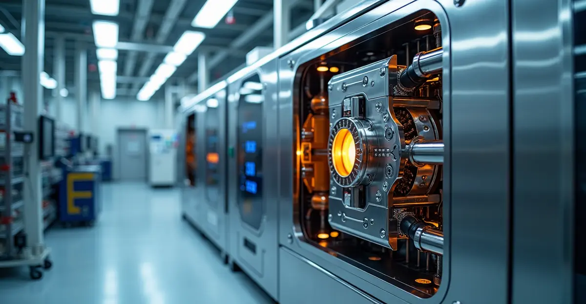
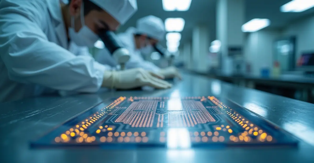
ASML's breakthrough centers on enhancing the light source in its EUV lithography machines, which are essential for manufacturing the world's most advanced semiconductors. The company achieved this by doubling the tin droplet rate to approximately 100,000 per second and implementing a dual-pulse laser system that shapes plasma more efficiently than previous single-pulse methods. 'This is no trick that works only in a specific setting for a short time,' said Michael Purvis, a top technologist at ASML, in an interview with Reuters. 'No, it's a system that can produce 1,000 watts under the same conditions as at a customer.'
Technical Specifications and Manufacturing Impact
The enhanced 1,000-watt EUV light source represents a 66% power increase over ASML's previous 600-watt systems. This advancement translates directly to manufacturing efficiency:
- Throughput Increase: From 220 wafers per hour to approximately 330 wafers per hour
- Cost Reduction: Lower production costs per chip for major foundries like TSMC, Intel, and Samsung
- Timeline: Full implementation expected by 2030 with gradual integration starting in 2027
- Future Roadmap: Clear path to 1,500 watts and potentially 2,000 watts in subsequent generations
How the Technology Works
EUV lithography uses 13.5-nanometer wavelength light to create intricate patterns on silicon wafers. The light is generated by firing high-powered lasers at microscopic tin droplets, creating plasma that emits extreme ultraviolet light. ASML's breakthrough involves precisely controlling this process with dual laser bursts and increased droplet frequency, allowing for more consistent and powerful light generation.
Strategic Importance in Global Semiconductor Competition
This technological advancement comes at a critical time in the global semiconductor race. ASML, which holds a virtual monopoly on EUV lithography systems, faces increasing pressure from both U.S. and Chinese competitors seeking to develop alternative technologies. The U.S.-China semiconductor trade war has intensified export restrictions on advanced chipmaking equipment, making ASML's continued technological leadership crucial for Western semiconductor independence.
'The light source is technologically the most challenging component of the most advanced machines,' according to Reuters analysis. With this breakthrough, ASML aims to maintain what company executives describe as an 'insurmountable lead' over potential challengers.
Competitive Landscape Analysis
| Competitor | Technology | Current Status | Estimated Timeline |
|---|---|---|---|
| ASML (Netherlands) | Laser-produced plasma EUV | Commercial production at 1,000W | Now available |
| Chinese R&D | Laser-induced discharge plasma | Prototype development | 2026-2027 trials |
| U.S. Initiatives | Alternative lithography approaches | Research phase | 2030+ target |
Geopolitical Implications and Export Restrictions
The breakthrough has significant geopolitical implications, particularly regarding export controls to China. Both the Biden and Trump administrations have pressured the Dutch government to restrict ASML's exports of advanced EUV systems to Chinese companies. This has created a situation where Chinese firms are investing heavily in domestic alternatives while American companies, with White House support, attempt to develop competing technologies.
The global semiconductor supply chain remains heavily dependent on ASML's technology, with the company's machines being essential for producing chips at 5nm nodes and below. This dependency has made ASML a focal point in international technology policy discussions.
Economic Impact and Industry Response
Major chip manufacturers have welcomed the development, which promises to lower their production costs while increasing output capacity. The timing is particularly important as demand for advanced semiconductors continues to grow across multiple sectors:
- AI Processors: Increased production capacity for next-generation AI chips
- Mobile Devices: More efficient manufacturing of smartphone processors
- Automotive: Enhanced capability for advanced driver-assistance systems
- Data Centers: Improved production of server and cloud computing chips
Future Outlook and Technological Roadmap
ASML has outlined a clear technological roadmap beyond the current 1,000-watt achievement. Company engineers see a path to 1,500 watts and potentially 2,000 watts in future iterations. This continuous improvement cycle is essential for maintaining Moore's Law—the observation that the number of transistors on a chip doubles approximately every two years.
The semiconductor manufacturing ecosystem will need to adapt to these advancements, with material suppliers, chemical companies, and equipment manufacturers all playing roles in supporting the increased throughput capabilities.
Frequently Asked Questions
What is EUV lithography?
Extreme ultraviolet lithography is a semiconductor manufacturing technology that uses 13.5-nanometer wavelength light to create intricate patterns on silicon wafers. It's essential for producing chips at 5nm nodes and below.
How much will chip production increase?
ASML estimates up to 50% more chips can be produced by 2030 with the new 1,000-watt light source, increasing from 220 to approximately 330 wafers per hour.
When will this technology be available?
The technology is being demonstrated now, with gradual implementation expected through 2027 and full deployment by 2030.
Why is this breakthrough important?
It maintains Western technological leadership in semiconductor manufacturing, lowers chip production costs, and addresses global chip supply challenges.
Will this affect chip prices?
Yes, increased manufacturing efficiency typically leads to lower production costs, which could eventually translate to more affordable advanced chips.
Sources
Reuters: ASML unveils EUV light source advance
Global Banking & Finance: ASML breakthrough details
TechPowerUp: Technical specifications
U.S. News: Competitive analysis


Follow Discussion