The 2026 Semiconductor Reconfiguration: How System-Level Innovation Is Replacing Traditional Node Scaling
The semiconductor industry is undergoing its most profound transformation since the invention of the integrated circuit, with system-level innovation through advanced packaging, chiplet architectures, and High Bandwidth Memory (HBM) now driving performance gains as traditional transistor scaling approaches physical limits. As the industry projects $975 billion in revenue by 2026, with advanced packaging contributing over 10% of TSMC's revenue, this fundamental shift is creating new strategic dependencies and reshaping global technology supply chains. The AI chip market explosion has accelerated this transition, with specialized chips for generative AI projected to exceed $150 billion by 2025 and approach $500 billion by 2026.
What Is System-Level Semiconductor Innovation?
System-level innovation represents a paradigm shift from focusing solely on shrinking transistor sizes (node scaling) to optimizing entire chip systems through advanced integration techniques. This approach combines multiple specialized components—processors, memory, accelerators—into cohesive systems using 2.5D and 3D packaging technologies. Unlike traditional monolithic designs where all functions reside on a single silicon die, system-level innovation leverages heterogeneous integration, allowing different components manufactured at different process nodes to work together seamlessly. This methodology addresses the diminishing returns of Moore's Law while delivering exponential performance improvements needed for AI workloads.
The Three Pillars of Semiconductor Reconfiguration
Advanced Packaging: The New Performance Frontier
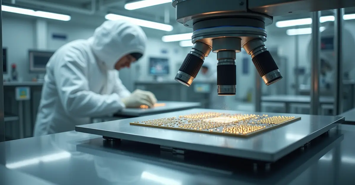
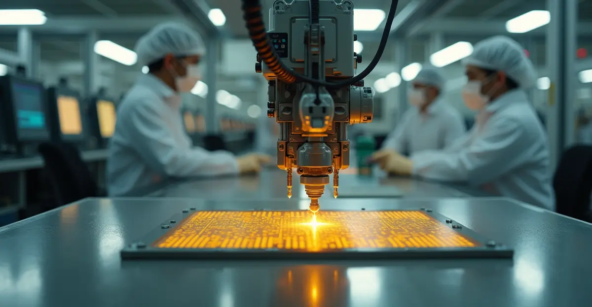
Advanced packaging technologies like TSMC's CoWoS (Chip-on-Wafer-on-Substrate) have become critical performance differentiators, experiencing 80% compound annual growth. These technologies enable multiple chips to communicate at unprecedented speeds by placing them side-by-side on silicon interposers. According to TechInsights' 2026 Advanced Packaging Outlook, co-packaged optics (CPO) will go mainstream as hyperscalers push for power savings in AI networking, with TSMC integrating COUPE into CoWoS. The company is expanding its advanced packaging footprint with two new CoWoS facilities in Chiayi Science Park expected to create 3,000 jobs, with mass production starting in 2026.
Chiplet Architectures: The LEGO Approach to Chip Design
Chiplet architectures represent a modular approach where small, functional circuit blocks are designed to be combined in mix-and-match fashion on interposers. This "LEGO-style" methodology allows companies to mix and match components from different manufacturers and process nodes, reducing development costs and time-to-market. The success of 2.5D assembly has given rise to chiplets, with several high-end products already taking advantage of these modular designs. Experts predict the emergence of an industry-wide chiplet ecosystem that could fundamentally change semiconductor design economics, similar to how the software component market revolutionized software development.
High Bandwidth Memory: Solving the AI Bottleneck
High Bandwidth Memory (HBM) has become essential for AI workloads, with demand projected to increase 40% from 2025 to 2026. HBM achieves higher bandwidth than traditional memory while using less power in a substantially smaller form factor by stacking up to eight DRAM dies vertically. The technology is experiencing unprecedented demand increases, with some prices exceeding 200% since early 2025 due to AI sector requirements. As noted in industry reports, "HBM is crowding out commodity DRAM capacity," with Micron noting a 3-to-1 conversion ratio between HBM and DDR5 wafer capacity, meaning every HBM ramp directly compresses general-purpose memory supply.
Global Supply Chain Implications
The shift to system-level innovation is creating new strategic dependencies in global technology supply chains. Taiwan's TSMC has secured a dominant position in advanced packaging, with NVIDIA securing the majority of its CoWoS capacity. This concentration creates potential bottlenecks in AI chip production, as all chips currently ship to Taiwan for packaging before distribution. The United States and China are racing to develop domestic capabilities, with Intel securing packaging customers including Amazon, Cisco, and recently commitments from Elon Musk's SpaceX, xAI and Tesla. The geopolitical semiconductor competition intensifies as these technologies become critical to national security and economic competitiveness.
Competitive Landscape: US, Taiwan, and China
The semiconductor reconfiguration is reshaping competitive dynamics between major players. TSMC maintains technological leadership with its CoWoS technology, but faces capacity constraints as demand surges. Intel, while technologically competitive, is building its packaging customer base and expanding operations. Chinese firms face significant challenges due to export restrictions on advanced packaging equipment, creating strategic vulnerabilities. The market is becoming increasingly bifurcated, with AI chips driving roughly half of total semiconductor revenue by 2026 despite representing less than 0.2% of total unit volume. This creates a two-speed market where traditional segments like automotive and consumer electronics see slower growth while AI segments experience explosive expansion.
National Security Considerations
Advanced packaging and chiplet technologies have become critical national security assets, with governments recognizing their strategic importance. The concentration of advanced packaging capabilities in Taiwan creates supply chain vulnerabilities, prompting initiatives like the US CHIPS Act to fund domestic development. Export controls on packaging equipment have become tools of technological competition, similar to restrictions on advanced lithography systems. As Dr. Robert Castellano notes in his analysis of TSMC's packaging surge, "The convergence of AI, high-bandwidth memory, and chiplet architectures has made advanced packaging a key performance differentiator in semiconductors" with implications for military and intelligence applications.
Expert Perspectives on the Transformation
Industry analysts emphasize the profound nature of this transition. "We're witnessing the most significant shift in semiconductor economics since the foundry model emerged," says a Deloitte semiconductor analyst. "System-level innovation through advanced packaging and chiplets is becoming more important than transistor scaling for many applications, particularly AI." TechInsights researchers note that thermal management challenges will intensify with 3D stacked architectures, driving adoption of liquid cooling and advanced thermal interface materials. Meanwhile, memory manufacturers face difficult allocation decisions as HBM demand competes with traditional DRAM production.
FAQ: Semiconductor System Innovation Explained
What is the difference between node scaling and system-level innovation?
Node scaling focuses on shrinking transistor sizes to pack more transistors onto a chip, while system-level innovation optimizes entire systems through advanced packaging, chiplet integration, and memory architectures. The former faces physical limits, while the latter offers new pathways to performance improvements.
Why is advanced packaging becoming so important?
Advanced packaging enables multiple chips to communicate at higher speeds with lower power consumption, addressing AI's massive data transfer requirements. Technologies like TSMC's CoWoS allow different components (processors, memory, accelerators) to work together as if they were a single chip.
How does the chiplet approach change semiconductor economics?
Chiplets allow companies to reuse proven designs across multiple products, reducing development costs and time-to-market. They enable mixing components from different manufacturers and process nodes, creating more flexible and cost-effective design approaches.
What are the supply chain risks of this transition?
The concentration of advanced packaging capabilities creates bottlenecks and strategic dependencies. Most advanced packaging occurs in Taiwan, creating geopolitical risks. Equipment restrictions and material shortages could disrupt the entire semiconductor ecosystem.
How will this affect AI chip development?
System-level innovation is essential for next-generation AI chips, which require massive memory bandwidth and efficient communication between specialized components. Advanced packaging and HBM enable the performance needed for large language models and other AI applications.
Future Outlook and Conclusion
The semiconductor industry's reconfiguration toward system-level innovation represents both a technological necessity and a strategic imperative. As traditional node scaling approaches physical and economic limits, advanced packaging, chiplet architectures, and High Bandwidth Memory offer new pathways to performance improvements. This transition is reshaping global supply chains, competitive dynamics, and national security considerations, with implications for economic and technological leadership in the AI era. Companies that master system-level integration will gain competitive advantages, while nations that develop domestic capabilities will enhance their technological sovereignty. The semiconductor manufacturing ecosystem is evolving from a focus on individual components to holistic system optimization, marking a fundamental shift in how computing performance is achieved and commercialized.
Sources
Deloitte 2026 Global Semiconductor Industry Outlook, TechInsights 2026 Advanced Packaging Outlook Report, TSMC and the Advanced Packaging Surge Analysis, CNBC Advanced Packaging Capacity Report, Wikipedia entries on 2.5D Integrated Circuits and High Bandwidth Memory.


Follow Discussion