The Advanced Packaging Arms Race: How Semiconductor Assembly Became the New Geopolitical Frontier
Advanced semiconductor packaging technologies have emerged as the latest critical battleground in the intensifying US-China technology competition, transforming what was once a back-end manufacturing process into a strategic geopolitical flashpoint. As the semiconductor industry shifts from traditional transistor miniaturization toward heterogeneous integration through chiplets, packaging capabilities have become as strategically vital as chip fabrication itself. With Bloomberg Intelligence projecting the advanced packaging market to reach $80 billion by 2033 amid explosive AI chip proliferation, recent US export controls targeting packaging equipment and China's accelerated domestic initiatives have elevated this previously overlooked segment to center stage in global technology sovereignty debates.
What is Advanced Semiconductor Packaging?
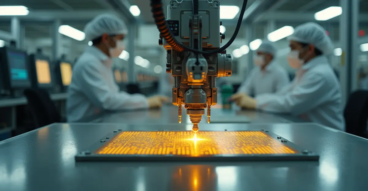
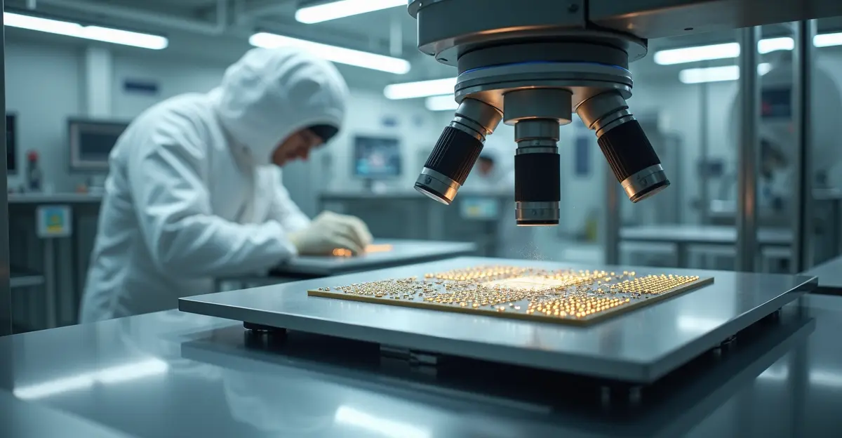
Advanced semiconductor packaging refers to sophisticated techniques that integrate multiple semiconductor dies, chiplets, and components into a single package using 2.5D and 3D stacking technologies. Unlike traditional packaging that simply protects individual chips, advanced packaging enables heterogeneous integration—combining different types of chips (logic, memory, analog) manufactured on different process nodes into unified systems. Key technologies include TSMC's CoWoS (Chip-on-Wafer-on-Substrate), Intel's Foveros, and various fan-out wafer-level packaging approaches. These methods dramatically improve performance, reduce power consumption, and enable continued progress as traditional Moore's Law scaling faces physical limitations.
The Geopolitical Context: From Manufacturing to Packaging
The strategic importance of advanced packaging has escalated dramatically since 2022, when the Biden administration implemented comprehensive export controls targeting China's access to advanced computing chips and chip-making equipment. According to a Congressional Research Service report, these controls aimed to limit China's military modernization and AI advancement by restricting high-performance computing capabilities. However, as noted in a CSIS analysis, these measures have created a 'double-edged sword' effect, accelerating Chinese efforts to 'design around' US technologies through domestic innovation in areas like advanced packaging.
This dynamic has transformed packaging from a manufacturing afterthought into a strategic priority. 'Advanced packaging has become crucial in the AI race between the US and China,' explains industry analysts, noting that technologies like CoWoS are essential for producing AI processors from companies like Nvidia and AMD. The global advanced packaging market, valued at $38.5 billion in 2024, is projected to grow at 11.5% CAGR to reach $111.4 billion by 2034, driven by AI, 5G, and automotive electronics demands.
US-China Competition: Export Controls and Domestic Initiatives
US Strategic Moves
The United States has increasingly targeted advanced packaging in its export control regime. While the Trump administration has softened some restrictions in 2026 to facilitate trade talks—approving higher-tier chip exports and suspending the 50% Affiliates Rule—enforcement actions continue. The Department of Commerce has intensified enforcement of existing rules, targeting loopholes like transshipment hubs and cloud service access. A $252 million fine against Applied Materials demonstrates this enforcement approach, maintaining pressure without directly disrupting trade negotiations.
TSMC's $100 billion investment in building advanced packaging facilities in Arizona represents a strategic move to create a complete US semiconductor supply chain from manufacturing to packaging. This reduces supply chain risks currently concentrated in Taiwan and strengthens US technological sovereignty in the face of growing US-China technology competition.
China's Domestic Push
China has responded with accelerated domestic packaging initiatives as part of its broader semiconductor self-reliance strategy. According to industry reports, China's semiconductor industry is undergoing a historic transformation in 2025, with companies like JCET Group expanding advanced packaging capabilities for AI and 5G chips. The upcoming Five-Year Plan represents a comprehensive national strategy to bolster China's semiconductor capabilities and reduce dependence on foreign technology.
A significant development occurred in February 2026 when SJ Semiconductor, a key player in China's advanced chip packaging sector, secured approval to list on Shanghai's STAR Market, aiming to raise 4.8 billion yuan (about $700 million). Founded through a strategic alliance between SMIC and JCET, SJ Semiconductor has achieved commercialization of 12-inch wafer-level chip packaging and scaled mass production of 2.5D and 3D packaging. Approximately 4 billion yuan from the IPO is earmarked for a 3D chip packaging project, positioning the company as China's first A-share listed firm primarily focused on wafer-level advanced packaging.
Technological Drivers: Chiplets and Heterogeneous Integration
The shift toward chiplet architectures and heterogeneous integration represents a fundamental transformation in semiconductor design. As traditional monolithic chip designs face physical and economic limitations, the industry is moving toward modular chiplet architectures that break down complex functionalities into smaller, specialized components. According to IDTechEx, the global chiplet market is projected to reach $411 billion by 2035, driven by high-performance computing demands in data centers and AI applications.
Key advantages of this approach include:
- Improved manufacturing yields through individual component testing
- Cost efficiency through optimal process node selection for different functions
- Enhanced performance and power efficiency through specialized components
- Greater scalability and ability to overcome lithography reticle limits
- Supply chain resilience through multi-supplier sourcing
Major industry players are embracing this approach, with AMD pioneering chiplet technology in its processors and AI accelerators, Intel developing chiplet-based processors through its IDM 2.0 strategy, and NVIDIA transitioning to chiplet designs with its Blackwell platform. The establishment of standards like Universal Chiplet Interconnect Express (UCIe) ensures interoperability and fosters a robust ecosystem for chiplet-based designs.
Market Dynamics and Strategic Implications
The advanced packaging market is experiencing explosive growth driven by AI demand. According to the 2025 Chiplets & Advanced Packaging Market Report, AI accelerator demand has outpaced advanced packaging capacity, with TSMC's CoWoS packaging fully booked through 2025 despite aggressive expansions. Chiplet architectures now drive over $40 billion in annual revenue, powering most high-end AI and HPC chips, with approximately 72% of AI accelerators using advanced multi-die packaging.
High-bandwidth memory (HBM) integration has surged, with HBM suppliers reporting 6-12 month lead times and prices jumping 20-30% year-on-year. NVIDIA alone is forecast to consume approximately 60% of global CoWoS capacity by 2026, highlighting the critical role of advanced packaging in meeting AI hardware demands. This concentration creates strategic vulnerabilities and opportunities in the ongoing global semiconductor supply chain competition.
Future Outlook: Next-Generation Technologies
The competition is rapidly advancing toward next-generation packaging technologies. According to TechInsights' 2026 Advanced Packaging Outlook Report, several key developments are expected:
- Co-packaged optics (CPO) will go mainstream as hyperscalers push for major power savings in AI networking, with TSMC integrating COUPE into CoWoS
- AI's appetite for HBM continues to exceed supply, with HBM4 and 16-Hi stacks rolling out, raising yield and thermal risks
- Glass substrates and panel-level packaging gain momentum as device sizes expand
- 3D stacked architectures intensify thermal challenges across AI, datacenter, and consumer markets
- Chiplet concepts may begin moving into mobile devices as shrinking form factors pressure traditional PoP designs
These technological advancements will further complicate the geopolitical landscape, as nations seek to secure leadership in critical enabling technologies that determine AI performance, military capabilities, and economic competitiveness.
Expert Perspectives and Industry Analysis
Industry analysts note that the advanced packaging competition represents a fundamental shift in semiconductor strategy. 'The packaging arms race reflects a broader recognition that technological leadership requires control over the entire semiconductor value chain,' observes one industry expert. 'As AI becomes increasingly dependent on heterogeneous integration, nations that master advanced packaging will have significant advantages in both commercial and military applications.'
The CSIS analysis warns that US export controls are creating unintended consequences by accelerating Chinese efforts to 'design out' and 'design around' US technologies. China's development of advanced packaging capabilities represents a key example of this 'design-around' trend, which threatens to shift the balance in US-China technology competition.
FAQ: Advanced Packaging Geopolitical Competition
What is advanced semiconductor packaging?
Advanced semiconductor packaging involves sophisticated techniques that integrate multiple semiconductor dies and components into single packages using 2.5D and 3D stacking technologies, enabling heterogeneous integration of different chip types.
Why has advanced packaging become geopolitically important?
Advanced packaging has become crucial for AI chip performance and military applications. As traditional chip scaling slows, packaging capabilities determine system performance, making them strategically vital in US-China technology competition.
What are the key technologies in advanced packaging?
Key technologies include TSMC's CoWoS, Intel's Foveros, fan-out wafer-level packaging, chiplet architectures, 3D stacking, and emerging approaches like co-packaged optics and glass substrates.
How is China developing domestic packaging capabilities?
China is accelerating domestic packaging through initiatives like SJ Semiconductor's IPO for 3D packaging projects, JCET Group's expansion, and strategic investments as part of its semiconductor self-reliance strategy under the Five-Year Plan.
What is the market outlook for advanced packaging?
The global advanced packaging market is projected to grow from $38.5 billion in 2024 to $111.4 billion by 2034, with Bloomberg Intelligence forecasting $80 billion by 2033, driven primarily by AI chip proliferation.
Conclusion: Reshaping Global Semiconductor Alliances
The advanced packaging arms race is fundamentally reshaping global semiconductor alliances, investment patterns, and technological sovereignty strategies. As nations recognize that packaging capabilities are as strategically important as chip fabrication, we are witnessing a reconfiguration of global supply chains and competitive dynamics. The competition extends beyond US-China rivalry to encompass Taiwan, South Korea, Japan, and European nations, each seeking to secure positions in this critical segment of the semiconductor value chain.
The outcome of this competition will have profound implications for AI development, military capabilities, and global economic leadership. As the industry continues its shift toward heterogeneous integration and chiplet architectures, mastery of advanced packaging technologies will increasingly determine which nations and companies can deliver the performance breakthroughs needed for next-generation computing. The packaging frontier has become, in essence, the new high ground in the global technology competition.
Sources
Congressional Research Service Report R48642, CSIS Analysis on Semiconductor Export Controls, CNN Technology Report 2025, TechInsights 2026 Advanced Packaging Outlook, IDTechEx Chiplet Technology Report 2025-2035, Bloomberg Intelligence Market Projections, TSMC Investment Announcements, SJ Semiconductor IPO Documentation, Industry Analyst Reports on US-China Technology Competition.


Follow Discussion