
What is the Imec Quantum Dot Qubit Breakthrough?
On May 19, 2026, at ITF World in Leuven, Belgium, imec — a world-leading research and innovation hub in advanced semiconductor technologies — announced a world first: a quantum dot qubit device fabricated using High NA EUV lithography. This achievement marks a critical milestone toward the industrial scaling of more reliable qubits, the basic computational units of quantum computers. By leveraging the most advanced lithography system originally developed for sub-2nm logic and memory chips, imec has demonstrated that silicon quantum dot spin qubits can be produced with unprecedented precision in a 300mm fab-compatible environment.
Background: Why Silicon Quantum Dot Spin Qubits Matter
Quantum computers promise exponential speedup for specific complex problems, such as drug discovery, materials science, and cryptography. However, building a useful quantum computer requires scaling to millions of connected qubits with high reliability and precise control. Among various quantum platforms, silicon quantum dot spin qubits — often called 'the industry qubits' — are considered a promising candidate for industrial scaling. Their production process is largely compatible with standard CMOS chip manufacturing, a domain where imec has built global authority over decades.
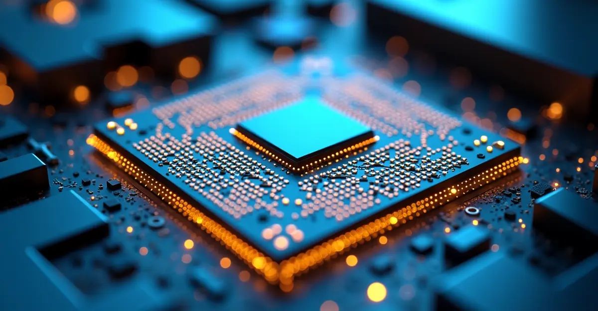
Silicon quantum dot spin qubits confine an individual electron within a silicon nanostructure. The 'spin state' of the trapped electron stores quantum information. To achieve reliable qubit operation, gaps between the various control gates must be minimized to reduce environmental noise. Imec has succeeded in fabricating a functioning network of qubits with gate gaps of barely 6 nanometers, enabled by High NA EUV lithography. This nanoscale precision theoretically allows millions of quantum bits to be integrated onto a single chip, a critical step toward practical quantum computers.
How High NA EUV Lithography Enables Qubit Scaling
High Numerical Aperture Extreme Ultraviolet (High NA EUV) lithography is the most advanced semiconductor patterning technology available. Developed by ASML, it is essential for manufacturing sub-2nm logic and high-density memory chips that fuel AI and high-performance computing. Imec has now shown that this same technology can be repurposed for quantum hardware.
Kristiaan De Greve, imec fellow and program director Quantum Computing, explained: 'High NA EUV enables the precise patterning of silicon quantum dot qubits. As the coupling strength between neighboring quantum dots increases exponentially with the gap between them, we need to reliably pattern gaps of a few nanometers between the control electrodes of the quantum dots. This is a true engineering feat, thanks to our integration and patterning teams and ASML's outstanding high NA EUV technology.'
This demonstration builds on imec's previous results with silicon quantum dot spin qubits, which already showed that CMOS-compatible processes can lead to low charge noise and stable qubit operation. By adding High NA EUV lithography, the focus shifts from individual demonstration devices in the lab to 300mm fab-compatible, reproducible quantum bits. The scaling of semiconductor manufacturing for quantum computing now appears within reach.
Technical Details of the Achievement
- Gate Gap: Imec achieved gaps of just 6 nanometers between plunger and barrier gates in a functioning qubit array.
- Qubit Type: Silicon quantum dot spin qubits, compatible with CMOS fabrication processes.
- Lithography Tool: High NA EUV lithography (provided by ASML) — the first integrated hardware device created with this technology.
- Scalability: The nanoscale precision enables theoretical integration of millions of qubits on a single chip.
- Fab Compatibility: The entire process runs on standard 300mm semiconductor manufacturing equipment.
Impact on the Quantum Computing Industry
This breakthrough accelerates the timeline for building useful quantum computers. By leveraging decades of semiconductor innovation, imec is moving quantum devices beyond lab experiments to large-scale, manufacturable systems. 'We can leverage decades of semiconductor innovation and reuse the entire ecosystem of silicon scaling, moving quantum devices beyond lab experiments to large-scale, manufacturable systems. This is where silicon-based qubits have a clear advantage,' said Sofie Beyne, project leader and quantum integration engineer at imec.
The achievement also highlights a growing convergence between traditional semiconductor manufacturing and quantum technology. High NA EUV lithography, previously seen as crucial only for classical computing, now plays a pivotal role in quantum hardware. This could accelerate investment in advanced lithography infrastructure and strengthen the business case for next-generation EUV tools. The future of quantum computing hardware increasingly depends on innovations from the semiconductor industry.
FAQ
What is a quantum dot qubit?
A quantum dot qubit is a quantum bit that confines an electron in a nanoscale semiconductor structure. The electron's spin state (up or down) represents quantum information, enabling quantum computations.
Why is High NA EUV lithography important for quantum computing?
High NA EUV lithography allows patterning of features just a few nanometers apart with extreme precision. For quantum dot qubits, smaller gaps between control electrodes dramatically improve qubit coupling and reliability, enabling scalable quantum chips.
How does this imec breakthrough compare to other quantum computing approaches?
Silicon spin qubits are considered 'industry qubits' because they can be manufactured using existing CMOS fabrication lines. This gives them a scalability advantage over superconducting or trapped-ion qubits, which require more exotic manufacturing processes.
When will practical quantum computers be available?
While this milestone is significant, scaling to millions of qubits remains a multi-year challenge. Imec's demonstration moves the technology from lab prototypes to fab-compatible production, but a fully fault-tolerant quantum computer is still likely a decade away.
What are the applications of quantum computing?
Quantum computers are expected to excel at drug discovery, materials simulation, cryptography, optimization problems, and complex financial modeling — tasks where classical computers struggle.
Sources
- Imec Press Release: World first: imec presents quantum dot qubit device using High NA EUV lithography
- Electronics For You: World's First High NA EUV Quantum Qubit Device
- New Electronics: Imec demonstrates quantum dot qubit fabricated with High NA EUV lithography
- The Quantum Insider: Imec Quantum Dot Qubit High NA EUV Lithography


Follow Discussion